ADC0804
The ADC0804 is a versatile chip that can be configured in many different ways, depending on how its pins are connected to each other and to external components. He we are showing the ADC0804 in a self-clocking mode by using an external RC timing network. The device is optimized for a clock around 600 kHz and requires approximately 64 clock cycles per conversion. The clock frequency may be figured by the following equation:fclk= 1 / (1.1 * R * C)
Does this equation ring any bells? It should, since it is very similar to an equation that you used to calculate the timing of 555 multivibrator circuits, which also used external RC timing networks.
Conversions are initiated by pulsing the chip's ~WR line (pin 3) low. The conversion cycle begins when this line goes high again. ~WR must then remain high during the conversion or the process will be abandoned. When the conversion is complete the ~INTR line (pin 5) produces a low pulse to indicate an end-of-conversion (EOC).
In this circuit we've tied ~INTR and ~WR together, so that as soon as one conversion is completed, another one is immediately begun. Differential analog voltage inputs allow offsetting the analog zero input voltage value. This means that the Vin(-) input (pin 7) can be used to automatically subtract a fixed voltage value from the input reading. In addition, the VREF/2 input (pin 9) can be adjusted to allow converting a smaller analog voltage span to the full 8 bits of resolution. In this experiment, the VREF/2 input will be set at 2.5 volts. Therefore our reference voltage VREF is equal to 5 V.
Build the following circuit:
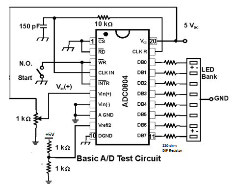
After the circuit is built:
To tell the chip to start performing conversions, momentarily close the switch (N.O. Start on diagram), then open the switch opened.
You should find that as you adjust the 1KΩ potentiometer, the LEDs change to show the digitized value of the input voltage.
More information on the ADC0804 can be found on the DATASHEET.